For both types of grid, lines between the grid points (marked by black dots in Figure 4.26) indicate that the points are to be connected by bidirectional delay lines. Connected points are separated by a distance ![]() . We will look at meshes of the type II form--that is, meshes for which we will need to calculate using only parallel junctions (recall that if we did not have losses or sources in (4.58a) and (4.58b) for the type II mesh of §4.4.2, the impedances of the bidirectional delay lines were set so that the series junctions degenerated to simple throughs) located at the grid points. We still allow
. We will look at meshes of the type II form--that is, meshes for which we will need to calculate using only parallel junctions (recall that if we did not have losses or sources in (4.58a) and (4.58b) for the type II mesh of §4.4.2, the impedances of the bidirectional delay lines were set so that the series junctions degenerated to simple throughs) located at the grid points. We still allow ![]() and
and ![]() to vary smoothly over the domain. Additionally, we could allow sources and losses in (4.58c), but as mentioned above, we consider only the fully lossless source-free case here. We remark that we now have a mesh for which all delays are of equal duration (i.e., in both connecting waveguides and self-loops), unlike the interleaved mesh of type I or III.
to vary smoothly over the domain. Additionally, we could allow sources and losses in (4.58c), but as mentioned above, we consider only the fully lossless source-free case here. We remark that we now have a mesh for which all delays are of equal duration (i.e., in both connecting waveguides and self-loops), unlike the interleaved mesh of type I or III.
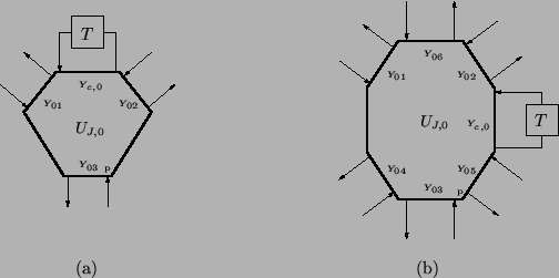
The derivation of the waveguide mesh equivalent difference schemes on a hexagonal or triangular grid is very similar to the rectilinear case, and we will omit most steps. Referring to Figure 4.26(a), for the hexagonal mesh we have a four-port parallel junction at each grid point. At grid point 0, for example, we have unit sample bidirectional delay lines connecting the junction to those at locations 1, 2, and 3, and we will name the admittances of the three connecting lines ![]() ,
, ![]() and
and ![]() respectively. In order to allow variation in local wave speed, we also add a self-loop of admittance
respectively. In order to allow variation in local wave speed, we also add a self-loop of admittance ![]() . The junction voltages at points 0, 1, 2, and 3 will be named
. The junction voltages at points 0, 1, 2, and 3 will be named ![]() ,
, ![]() ,
, ![]() and
and ![]() , and we have, for the junction admittance at point 0,
, and we have, for the junction admittance at point 0,
Beginning at junction 0, and performing manipulations similar to those on a rectilinear grid (i.e., breaking the junction voltage into wave components, and tracing their movement through the network), we get a difference relation among the voltages at point 0 and its neighbors:
 |
The stability bound for this mesh, resulting from a positivity condition on the self-loop admittance ![]() over all grid points
over all grid points ![]() is
is
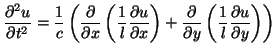
The approach to the triangular mesh is very similar. We now have, at each grid point, a seven-port junction, to accommodate waves incoming from six directions and a self-loop (see Figure 4.27(b)). We now make the choices, at a grid point 0, of
 |
If ![]() and
and ![]() are constant, and we are operating at the CFL bound (i.e.,
are constant, and we are operating at the CFL bound (i.e.,
![]() ), then in both the hexagonal or the triangular meshes
), then in both the hexagonal or the triangular meshes ![]() vanishes, and we have, respectively, three-port and six-port scattering junctions, all of whose port admittances are identical. These meshes, although they are slightly more difficult to program than the rectilinear mesh, possess better numerical dispersion properties [157]; a comparison of the directional dispersion of various types of (2+1)D meshes in the constant-coefficient case is given in §A.2. We also note that in this same constant-coefficient case, when we are at CFL, the hexagonal mesh, like the rectilinear mesh, can be decomposed into two meshes which operate on half the grid points, and thus a cut in computational and memory costs of a factor of two is possible (see §4.4.3). This is not true for the triangular mesh--see Appendix A.
vanishes, and we have, respectively, three-port and six-port scattering junctions, all of whose port admittances are identical. These meshes, although they are slightly more difficult to program than the rectilinear mesh, possess better numerical dispersion properties [157]; a comparison of the directional dispersion of various types of (2+1)D meshes in the constant-coefficient case is given in §A.2. We also note that in this same constant-coefficient case, when we are at CFL, the hexagonal mesh, like the rectilinear mesh, can be decomposed into two meshes which operate on half the grid points, and thus a cut in computational and memory costs of a factor of two is possible (see §4.4.3). This is not true for the triangular mesh--see Appendix A.
We do not include any material about boundary termination of hexagonal or triangular grids, although we do conjecture that it should be comparatively less tricky than the termination of MDWDF networks in the same coordinate systems (we mentioned a hexagonal coordinate system in passing in §3.3.3), where the available results are extremely unsatisfactory [211,212].