Next: Losses, Sources, and Spatially-varying
Up: The (2+1)D Parallel-plate System
Previous: Defining Equations and Centered
The Waveguide Mesh
Consider the original form (2+1)D waveguide network, or mesh [198], operating on a rectilinear grid. Each scattering junction (parallel) is connected to four neighbors by unit sample bidirectional delay lines. The spacing of the junctions is  (in either the
  or
or  direction) and the time delay is
  in the delay lines (see Figure 4.19). We now index a junction (and all its associated voltages and currents and wave quantities) at coordinates
 by the pair
  .
.
Figure 4.19:
(2+1)D waveguide mesh and a representative scattering junction.
 |
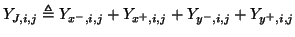
As in the (1+1)D case, at each parallel junction at location , we have voltages at every port, given by
 |
 |
voltage in waveguide leading east |
|
 |
|
voltage in waveguide leading west |
|
 |
|
voltage in waveguide leading north |
|
 |
|
voltage in waveguide leading south |
|
and current flows
 |
|
current flow in waveguide leading east |
|
 |
|
current flow in waveguide leading west |
|
 |
|
current flow in waveguide leading north |
|
 |
|
current flow in waveguide leading south |
|
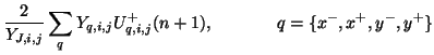
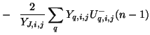
as well as wave quantities
where  is any of
  ,
,  ,
,  or
or  . The variables superscripted with a
  refer to the incoming waves, and those marked
  to outgoing waves. The voltage and current waves are related by
 |
(4.67) |
where  is the admittance of the waveguide connected to the junction with coordinates
in direction . The junction admittance is then
is the admittance of the waveguide connected to the junction with coordinates
in direction . The junction admittance is then
 |
(4.68) |
and the scattering equation, for voltage waves, will be, from (4.15),
 |
(4.69) |
where  is any of , , , or .
Voltage waves are propagated by:
is any of , , , or .
Voltage waves are propagated by:
The case of flow waves is similar except for a sign inversion. The complete picture is shown in Figure 4.19.
Similarly to the (1+1)D case, it is possible to obtain a finite difference scheme purely in terms of the junction voltages  , under the assumption that the admittances of all the waveguides in the network are identical, and equal to some positive constant
  . Thus, from (4.56),
 . We have, for the junction at location
  ,
,  ,
,
This is identical to
 if we replace
  by
by  .
.
If we now replace all the bidirectional delay lines in Figure 4.19 by the same split pair of lines shown in Figure 4.11, then we get the arrangement in Figure 4.20.
Figure 4.20:
(2+1)D interleaved waveguide mesh.
 |
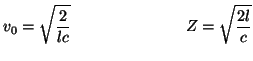
We have placed the split lines such that the branches containing sign inversions are adjacent to the western and southern ports of the parallel junctions. We also introduce new junction variables  at the series junctions between two horizontal half-sample waveguides, and
  at the series junctions between two vertical delay lines, as well as all the associated wave quantities at the ports of the new series junctions. It is straightforward to show that upon identifying , and with
  and
and  and , the mesh will calculating according to scheme (4.52) with constant coefficients, if we choose
where  is the impedance in all the delay lines. We are again at the magic time step, but the impedance has been set to be larger than the characteristic impedance of the medium. Also, notice that the speed of propagation along the delay lines is not the wave speed of the medium, which is
 . Such a mesh is called a slow-wave structure [90] in the TLM literature. At this point, it is useful to compare Figures 4.20 and 4.18.
Subsections
Next: Losses, Sources, and Spatially-varying
Up: The (2+1)D Parallel-plate System
Previous: Defining Equations and Centered
Stefan Bilbao
2002-01-22