next up previous
Next: Vector Waveguides and Scattering Up: Digital Waveguides Previous: Note on the Different

Scattering Junctions

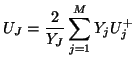
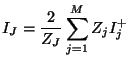
Returning to the ``input-output'' waveguide defined in §4.2.1 and §4.2.2, we now must deal with connecting bidirectional delay lines; this is done in the same way as in the wave digital filtering framework, namely through the use of Kirchoff's Laws, which conserve instantaneous power at a connection. The resulting equations relating input to output waves at such a connection or scattering junction are identical to the adaptor equations for wave digital filters already mentioned in §2.3.5. For completeness sake, we will re-derive the scattering equations for a series connection of $ M$ bidirectional delay lines, of impedances $ Z_{j}$, $ j=1,\hdots,M$.

At such a series connection, we must have

$\displaystyle I_{1}$ $\displaystyle = I_{2}$   $\displaystyle = \hdots$   $\displaystyle = I_{M}$   $\displaystyle \triangleq I_{J}$ (4.12)
$\displaystyle U_{1}$ $\displaystyle + U_{2}$   $\displaystyle + \hdots$   $\displaystyle +U_{M}$   $\displaystyle =0$ (4.13)

where $ I_{J}$ is defined to be the junction current common to all waveguides.

Thus, we have

$\displaystyle 0 \stackrel{\eqref{wgsereq2}}{=} \sum_{j=1}^{M}U_{j}\stackrel{\eq...
...stackrel{\eqref{physcureq}}{=} \sum_{j=1}^{M}Z_{j}\left(2I_{j}^{+}-I_{j}\right)$    

where the equation numbers appear over the equalities to which they pertain. Using (4.12), we can then write the equation used to calculate the junction current from the incoming current waves

$\displaystyle I_{J} = \frac{2}{Z_{J}}\sum_{j=1}^{M}Z_{j}I_{j}^{+}$    

as well as the scattering equation

$\displaystyle I_{k}^{-} = -I_{k}^{+}+\frac{2}{Z_{J}}\sum_{j=1}^{M}Z_{j}I_{j}^{+},\hspace{0.5in}k=1,\hdots, M$    

where we have defined the junction impedance $ Z_{J}$ by

$\displaystyle Z_{J} \triangleq \sum_{j=1}^{M}Z_{j}$    

In terms of voltage waves, using (4.4a) and (4.4b), the scattering equations can be written as

$\displaystyle U_{k}^{-} = U_{k}^{+}-\frac{2Z_{k}}{Z_{J}}\sum_{j=1}^{M}U_{j}^{+},\hspace{0.5in}k=1,\hdots, M$    

This is identical to the definition of a wave digital series adaptor (2.31) for voltage waves, where we replace $ U_{k}^{-}$ by $ b_{k}$, $ U_{k}^{+}$ by $ a_{k}$ and $ Z_{k}$ by $ R_{k}$, for $ k=1,\hdots,M$.

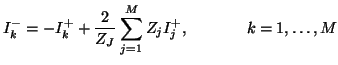
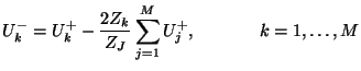
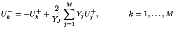
The scattering equations for a dual parallel connection are similar under the replacement of $ U_{k}^{+}$ and $ U_{k}^{-}$ by $ I_{k}^{+}$ and $ I_{k}^{-}$, $ Z_{k}$ by $ Y_{k}$ and $ Z_{J}$ by the junction admittance, defined by

$\displaystyle Y_{J} \triangleq \sum_{j=1}^{M}Y_{j}$    

so that we have

$\displaystyle U_{J} = \frac{2}{Y_{J}}\sum_{j=1}^{M}Y_{j}U_{j}^{+}$ (4.14)

and

$\displaystyle U_{k}^{-} = -U_{k}^{+}+\frac{2}{Y_{J}}\sum_{j=1}^{M}Y_{j}U_{j}^{+},\hspace{0.5in}k=1,\hdots, M$ (4.15)

The representation we will use for scattering junctions in the waveguide networks in this and the subsequent chapter will usually be as shown in Figure 4.3 (in the case of a connection of four waveguides).

Figure 4.3: Graphical representations of scattering 4-port junctions-- (a) series and (b) parallel.
\begin{figure}\begin{center}
\begin{picture}(380,160)
% graphpaper(0,0)(380,160...
...(a)}
\put(300,-60){(b)}
\end{picture} \end{center} \vspace{0.5in}
\end{figure}

A waveguide's immittance is placed at the port at which it is connected to the junction, and the junction quantity to be calculated from incoming waves appears at the center of the junction. Sometimes, if there is no room in the figure, we will indicate the immittance of a waveguide by an overbrace (see, e.g., Figure 4.8). In the case of electrical variables, a junction current $ I_{J}$ is calculated at a series junction, and a junction voltage $ U_{J}$ at a parallel junction, but when we move to mechanical systems in the next chapter, we will of course use different variable names. A small ``s'' or ``p'' is placed in a corner of the junction in order to indicate that the junction is series or parallel, respectively. In addition, because it is only necessary to propagate one type of wave in a bidirectional delay line, a graphical representation of a waveguide network will always imply the use of voltage waves everywhere. This is the same convention that is used in wave digital signal flow graphs. This is important, because it will be recalled from §4.2.2 that current waves require an additional sign inversion that is not shown in the network diagrams.

Instantaneous power is preserved at the scattering junction (here again, as in the WDF case, the scattering junction is no more than a wave variable implementation of Kirchoff's Laws, which preserve power by definition). The power-normalization strategy employed in the wave digital filter setting can also be used here as well, and gives rise to the same orthogonality property of the scattering junction in either the series or parallel case (see §2.3.5). Power-normalized waves can be used in order to construct time-varying passive waveguide networks [165], though for time-invariant problems, the use of such power-normalized quantities involves more arithmetic operations.


next up previous
Next: Vector Waveguides and Scattering Up: Digital Waveguides Previous: Note on the Different
Stefan Bilbao 2002-01-22