


Next: Waveguide Network and the
Up: The (1+1)D Transmission Line
Previous: Centered Difference Schemes and
Consider the waveguide network pictured in Figure 4.8. Each scattering junction (in this case parallel) is connected to its two neighbors by unit sample bidirectional delay lines. The spacing of the junctions is  and the waveguide delays are of duration
  . The voltage at a junction with coordinate
  and at time
  is denoted by
 for integer
  and
and 
 .
.
Figure 4.8:
(1+1)D waveguide network.
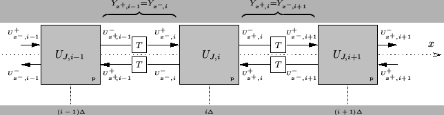 |
We can name the voltages and current flows in individual waveguides in the following way. At junction , the line voltages are:
| |
 |
|
 voltage in waveguide leading east voltage in waveguide leading east |
|
| |
 |
|
voltage in waveguide leading west |
|
and the flows are:
| |
 |
|
current flow in waveguide leading east |
|
| |
 |
|
current flow in waveguide leading west |
|
The constraints, imposed by Kirchoff's Laws at a parallel junction, are:
 |
(4.25) |
As discussed in §4.2, the voltages and current flows in the individual waveguides can be further broken up into incoming and outgoing waves. That is, we have, at a junction at grid location :
where  is either of
  or
or  . The variables superscripted with a
  refer to the incoming waves, and those marked
  to outgoing waves. In a particular waveguide section, the current and voltage waves are related by:
 |
(4.26) |
where  is the characteristic admittance of the waveguide connected to junction in direction . In addition, because the junctions at and
  are connected to opposite ends of the same waveguide, we have
As before, we will also define the impedance of any waveguide to be
At a particular parallel junction, the junction admittance will thus be
In this case, from (4.14), the junction voltage can be written in terms of incoming wave variables as
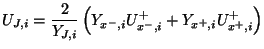 |
(4.27) |
and the outgoing voltage waves from any junction are related to the incoming waves by
where  refers to either of the directions or .
The incoming voltage wave entering each junction from a particular waveguide at time step is simply the outgoing voltage wave leaving a neighboring junction, one time step before. Reading directly from Figure 4.8, we have
 |
(4.28a) |
The case of flow waves is similar except for a sign inversion--that is, we have
 |
(4.29a) |
As discussed in §4.2, we can perform all calculations using voltage waves; in the waveguide networks pictured in this chapter, we will always assume, without loss of generality, that we are dealing with voltage waves.
Next: Waveguide Network and the
Up: The (1+1)D Transmission Line
Previous: Centered Difference Schemes and
Stefan Bilbao
2002-01-22