Next: The Unit Element
Up: Wave Digital Elements and
Previous: Pseudopower and Pseudopassivity
Wave Digital Elements
We will now present the wave digital equivalents of all the circuit elements mentioned in §2.2.4.
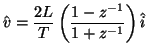
Under the bilinear transform (2.11), the steady-state equation for an inductor becomes
or, in the discrete-time domain,
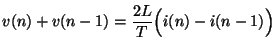
Applying the definition of wave variables (2.14), we get, in the time domain,
 |
(2.22) |
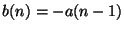
If we make the choice
then (2.22) simplifies to
 |
(2.23) |
Thus the input wave  must undergo a delay and sign-inversion before it is output as
  . In terms of steady-state quantities, we have
 |
(2.24) |
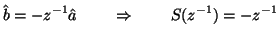
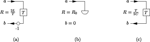
The reflectance  is, as expected, LBR (see previous section). The resulting wave digital one-port is shown in Figure 2.7(a).
The derivations of the wave digital one-ports corresponding to the resistor and capacitor are similar; their signal-flow graphs also appear in Figure 2.7. We note that the same choice of the port resistance  should be made in the case of power-normalized wave variables. We also note in passing that we have used here the symbol
  to represent a unit delay in a wave digital filter
 .
.
Figure 2.7:
Wave digital one-ports corresponding to the classical one-ports of Figure 2.3-- (a) the wave digital inductor, (b) resistor, and (c) capacitor.
 |
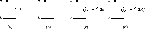
The short-circuit and open-circuit one-ports are, for any choice of the port resistance , perfectly reflecting (with or without sign inversion, respectively). The appearance of the factor in the definition of the wave digital current source results from our choice of using voltage waves (as opposed to current waves). In all the wave digital one-ports of Figure 2.8, there is an instantaneous dependence of the output wave on the input wave , and we may expect delay-free loops to appear when these elements are connected with others. On the other hand, the form of these one-ports does not depend on a particular choice of the port resistance (except in a very minor way for a current source), and remains a free parameter, which can be used, in many cases, to remove delay-free loops.
Figure 2.8:
Wave digital one-ports corresponding to the classical one-ports of Figure 2.4-- (a) short-circuit, (b) open-circuit, (c) voltage source and (d) current source.
 |
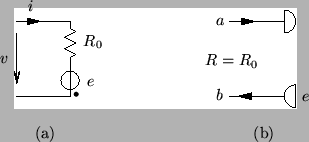
It is also possible to combine resistances and sources [46]; a resistive voltage source, shown in Figure 2.9(a), consists of a voltage source  in series with a resistor of resistance
  . If the port resistance of the combined one-port is chosen to be , then the wave digital one-port [46] is as shown in Figure 2.9(b). A wave digital resistive current source can be similarly defined.
Figure 2.9: (a) A resistive voltage source, and (b) the associated wave digital one-port.
 |
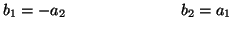
The classical transformer and gyrator two-ports can be treated in the same way. For example, the gyrator accepts two input waves  and
and  , and yields two output waves
  and
and  . There are two port resistances,
  and
and  . The instantaneous equations (2.10) relating the voltages and currents in a gyrator become, upon substitution of wave variables,
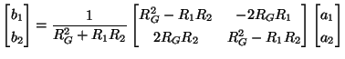 |
(2.25) |
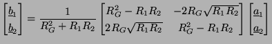
which simplifies, under the choice of
 and
and
 to
to
 |
(2.26) |
If we are using power-normalized wave variables, then the scattering equation for the gyrator becomes
 |
(2.27) |
In this case, any choice of the port resistances such that
 gives
gives
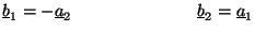 |
(2.28) |
The ideal transformer also can take on various forms, depending on the choices of the port resistances and on the type of wave variable employed. Under a choice of port resistances and such that
 , the equations (2.9) for the ideal transformer of turns ratio
  become
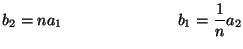 |
(2.29) |
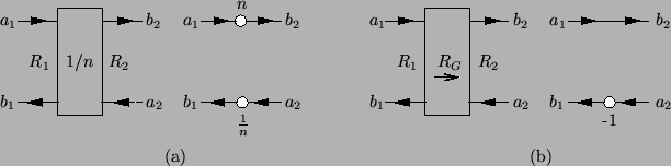
For the transformer and gyrator WD two-ports, we adopt general symbols that do not reflect a particular choice of the port resistances. If simplifying choices can be made in either case, than we can write the signal flow graph explicitly (see Figure 2.10). There may be occasions when it is not be possible to make these simplifying choices of the port resistances which yield (2.26) and (2.29). For example, when we approach the numerical integration of beam and plate systems in Chapter 5, as well as certain balanced forms (see §3.12) the WD networks contain gyrators whose port resistances are constrained, forcing us to use (2.25).
Figure 2.10:
Wave digital two-ports-- (a) a transformer with turns ratio and its simpler form for
and (b) a gyrator of gyration coefficient  and its simpler form for
 .
.
 |
We also mention that these two-ports are both lossless, and in fact non-energic [42] (i.e., we have
 , for all ).
Numerous other wave digital elements have been proposed, namely circulators, quasi-reciprocal lines (QUARLS), as well as unit elements [46]. All have been applied fruitfully to filter design problems, but the unit element deserves a special treatment.
Subsections
Next: The Unit Element
Up: Wave Digital Elements and
Previous: Pseudopower and Pseudopassivity
Stefan Bilbao
2002-01-22