The element values ![]() ,
, ![]() ,
, ![]() and
and ![]() are the same as before, except scaled by a factor
are the same as before, except scaled by a factor ![]() , and the capacitance value will be
, and the capacitance value will be
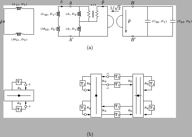
The resulting MD digital network is shown in Figure B.3(b). As before, the two-port ![]() transforms to a pair of bidirectional delay lines under the application of the spectral mappings defined by (4.107). The other circuit elements, namely the nonlinear inductors and capacitors, must be discretized using the trapezoid rule, and so we are left with a network which is neither an MDWDF nor a DWN, but which contains elements of both. The port resistance are determined in the usual way; for an inductance
transforms to a pair of bidirectional delay lines under the application of the spectral mappings defined by (4.107). The other circuit elements, namely the nonlinear inductors and capacitors, must be discretized using the trapezoid rule, and so we are left with a network which is neither an MDWDF nor a DWN, but which contains elements of both. The port resistance are determined in the usual way; for an inductance ![]() and direction
and direction ![]() , by
, by
![]() and for a capacitance
and for a capacitance ![]() of direction
of direction ![]() by
by
![]() . The port resistances of the paired multidimensional unit elements will be
. The port resistances of the paired multidimensional unit elements will be
![]() .
.
 |
It would be possible to choose the directional shift lengths in the one-port inductances and capacitances differently from those in the unit elements such that the network could conceivably operate in an interleaved (offset) configuration; parallel junctions which calculate ![]() alternate with series junctions calculating
alternate with series junctions calculating ![]() . A potential problem here is that the port resistances at the parallel junctions (say) depend on
. A potential problem here is that the port resistances at the parallel junctions (say) depend on ![]() , but
, but ![]() are not calculated at these grid locations; some approximation is thus necessary, but we do not pursue the matter further here.
are not calculated at these grid locations; some approximation is thus necessary, but we do not pursue the matter further here.