Next: Other Waveguide Networks for
Up: Timoshenko's Beam Equations
Previous: MDKC and MDWDF for
Waveguide Network for Timoshenko's System
Recall, from §4.10, that for the (1+1)D transmission line problem, it is possible to obtain a DWN from an MDKC after a few network manipulations, and under the application of an alternative spectral mapping, or integration rule. We may proceed in the same way for Timoshenko's system, and we will skip most of the steps that were detailed in the earlier treatment. We do recall, however, that the original system of equations should be scaled by a factor of  , the grid spacing, before making the switch to DWNs.
We first transform the MDKC of Figure 5.5 such that the quantities  and
and  represent voltages across capacitors, instead of currents through inductors. The transformed MDKC is shown in Figure 5.7.
Figure 5.7:
Transformed MDKC for Timoshenko's system.
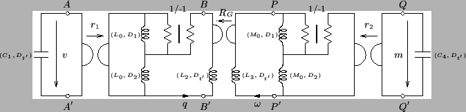 |
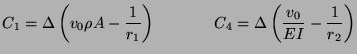
The inductances are all as in Figure 5.5, except scaled by , and the new capacitance values will be
and the gyration coefficient  will be equal to .
As before, it is possible to interpret the two two-ports
will be equal to .
As before, it is possible to interpret the two two-ports  and
and  as MD representations of digital waveguide pairs, if we apply the alternative spectral mapping or integration rule as in §4.10. The MD waveguide network is shown in Figure 5.8.
Figure 5.8:
Waveguide network for Timoshenko's system, in a multidimensional form.
|
|
Here we have chosen the step sizes such that an interleaved algorithm results, just as for the transmission line problem, as discussed in §4.10. Thus, we have
 and
and
 so that in a computer implementation, approximations to and are alternated with those of
  and
and  . The signal flow diagram corresponding to Figure 5.8 is shown, as a DWN, in Figure 5.9.
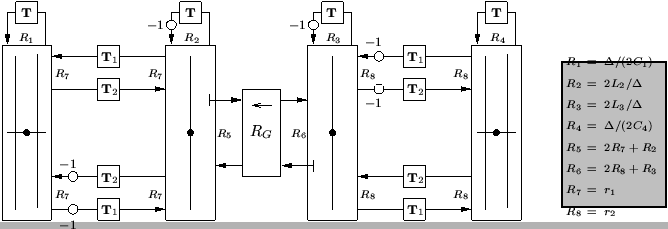
Figure 5.9:
DWN for Timoshenko's system.
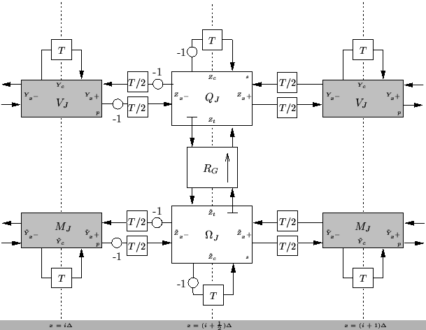 |
The junction quantities  ,
,  ,
,
 and
and  approximate , , and respectively and for consistency with the DWN notation of Chapter 4, we have replaced the port resistances by waveguide admittances (at the parallel junctions) and impedances (at the series junctions). Because there are now two sets of immittances at any grid point (corresponding to the upper and lower rails in Figure 5.9), we have indexed half of them with a tilde. Referring to Figure 5.9, the self-loop immittances will be given by
at alternating grid locations indexed by integer  . The connecting immittances will be, referring to the series junctions,
The DWN incorporates a gyrator between the two series junctions, and as such, we must employ reflection-free ports at at least one of the two connected junction ports. Though reflection-free ports and gyrators have not as yet appeared in the DWN context, it is straightforward (indeed immediate, if we are considering DWNs derived from MDKCs), to transfer them from wave digital filters. These port impedances (subscripted with a  ) at the series junctions can be chosen to be
This is a structure of the type III form (i.e., the connecting immittances are spatially invariant; see §4.3.6), and the bound on  is suboptimal (and the same as that for the MDWDF structure discussed in the last section). The possible interleaving of the calculated junction quantities in this structure is indicated, as in Chapter 4, by grey/white coloring of scattering junctions.
Next: Other Waveguide Networks for
Up: Timoshenko's Beam Equations
Previous: MDKC and MDWDF for
Stefan Bilbao
2002-01-22