 |
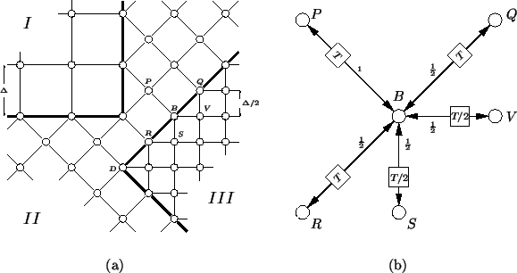
Consider the grid arrangement of Figure 4.38(a). The interface between region ![]() and region
and region ![]() was discussed in the previous section; in that case, we assumed the waveguide delays to be identical everywhere in regions
was discussed in the previous section; in that case, we assumed the waveguide delays to be identical everywhere in regions ![]() and
and ![]() , including the boundary. We can, of course, apply the same idea again in order to introduce a grid of quadrupled point density, by adjoining it to region
, including the boundary. We can, of course, apply the same idea again in order to introduce a grid of quadrupled point density, by adjoining it to region ![]() . In this case, however, we would like to take advantage of the fact that waveguide lengths in region
. In this case, however, we would like to take advantage of the fact that waveguide lengths in region ![]() are half those of region
are half those of region ![]() ; it is more natural, then, to use a delay of half that of region
; it is more natural, then, to use a delay of half that of region ![]() throughout the interior of region
throughout the interior of region ![]() . Waveguides which run along the boundary will still operate at the rate of regions
. Waveguides which run along the boundary will still operate at the rate of regions ![]() and
and ![]() , as will the self-loop (of admittance
, as will the self-loop (of admittance ![]() , not shown). A scattering junction at a typical point
, not shown). A scattering junction at a typical point ![]() on the boundary between regions
on the boundary between regions ![]() and
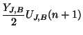
and ![]() is shown in Figure 4.38(b). Here, we have abbreviated the depiction of a bidirectional delay line to a single double-headed arrow, and have omitted the self-loop (which contains a full unit delay). Note in particular that for such a boundary junction, the delays of the connecting waveguides are now not all identical. As might be expected, the difference scheme relating the junction voltage at such a point to those of its neighbors is no longer a simple two-step difference method, but a four-step scheme, where each time step is now
is shown in Figure 4.38(b). Here, we have abbreviated the depiction of a bidirectional delay line to a single double-headed arrow, and have omitted the self-loop (which contains a full unit delay). Note in particular that for such a boundary junction, the delays of the connecting waveguides are now not all identical. As might be expected, the difference scheme relating the junction voltage at such a point to those of its neighbors is no longer a simple two-step difference method, but a four-step scheme, where each time step is now
![]() ; a full derivation of this difference scheme is very lengthy but rewarding, in the sense that it becomes clear why it takes four steps for the wave variables to fully ``recombine'' into junction voltages. We will, however, only present the resulting difference equation for a boundary junction at location
; a full derivation of this difference scheme is very lengthy but rewarding, in the sense that it becomes clear why it takes four steps for the wave variables to fully ``recombine'' into junction voltages. We will, however, only present the resulting difference equation for a boundary junction at location ![]() as in Figure 4.38(b). Here the junction voltage will be
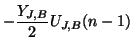
as in Figure 4.38(b). Here the junction voltage will be ![]() , and the junction voltages at the neighboring points are, referring to Figure 4.38(b),
, and the junction voltages at the neighboring points are, referring to Figure 4.38(b),
![]() . The admittances of the connecting waveguides will be called
. The admittances of the connecting waveguides will be called
![]() , the self-loop admittance
, the self-loop admittance ![]() and the junction admittance at point
and the junction admittance at point ![]() is defined as
is defined as
We have
 |
||||
 |
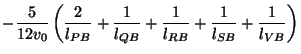
Because we now have a four-step scheme, the determination of ![]() is no longer as simple as in the two-step case, but it can be found, nevertheless, to be
is no longer as simple as in the two-step case, but it can be found, nevertheless, to be
 |
The positivity requirement yields the bound
![$\displaystyle v_{0}\geq \max_{\begin{minipage}[t]{1.0in}\begin{center}\tiny {II/III boundary waveguide midpoints}\end{center}\end{minipage}}\sqrt{\frac{10}{3lc}}$](img2060.png) |
Corners present essentially the same problems as before, and we will not discuss them further, other than to repeat that, given the settings derived above for the waveguide admittances at the ![]() /
/![]() boundary, which determine completely the scattering behavior at the corners (an example of which is point
boundary, which determine completely the scattering behavior at the corners (an example of which is point ![]() in Figure 4.38(a)), the mesh will not be consistent with the parallel-plate system at these points.
in Figure 4.38(a)), the mesh will not be consistent with the parallel-plate system at these points.