 |
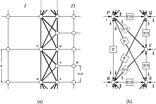
Instead of progressing, in two steps, from a grid to one of quadrupled point density, as we did in the last section, we might ask whether it is possible to design a direct passive interface in order to quadruple grid density in one step. Such an arrangement is shown in Figure 4.39(a): a quadrupled density region (![]() ), for which the delay in all waveguides is one-half time step, or
), for which the delay in all waveguides is one-half time step, or
![]() is adjoined to a rectilinear mesh (
is adjoined to a rectilinear mesh (![]() ) via a matching layer composed of various waveguides connecting each point on the boundary of region
) via a matching layer composed of various waveguides connecting each point on the boundary of region ![]() with five neighboring points in region
with five neighboring points in region ![]() . The admittances and delays of the waveguides in the matching layer must be set to particular values relative to the values in the interiors of regions
. The admittances and delays of the waveguides in the matching layer must be set to particular values relative to the values in the interiors of regions ![]() and
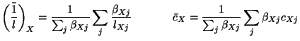
and ![]() so as to satisfy the transmission line equations at all grid points (junctions). These delays and admittance settings are shown in Figure 4.39(b), where we have used the following notation for the admittance settings: first suppose that admittances in the interior of region
so as to satisfy the transmission line equations at all grid points (junctions). These delays and admittance settings are shown in Figure 4.39(b), where we have used the following notation for the admittance settings: first suppose that admittances in the interior of region ![]() are set to the normal values for a type II mesh--namely, the admittance of a particular connecting waveguide is equal to
are set to the normal values for a type II mesh--namely, the admittance of a particular connecting waveguide is equal to
![]() , where
, where ![]() is evaluated at the midpoint of the waveguide. All other connecting admittances in the network, including those in region
is evaluated at the midpoint of the waveguide. All other connecting admittances in the network, including those in region ![]() and in the matching later, will also be set to
and in the matching later, will also be set to
![]() , where
, where ![]() is evaluated at the center of the particular waveguide, and multiplied by a scaling coefficient. In Figure 4.39(b), this scaling coefficient is shown next to the waveguide. For example, for the waveguide connecting point
is evaluated at the center of the particular waveguide, and multiplied by a scaling coefficient. In Figure 4.39(b), this scaling coefficient is shown next to the waveguide. For example, for the waveguide connecting point ![]() to point
to point ![]() , the admittance should be set to
, the admittance should be set to
It is simple (after some tedious algebra) to set the self-loop admittances at the junctions in the matching layer such that the transmission line equations are approximated at these points. We first define average capacitances and inverse inductances at a junction at point ![]() by:
by:
 |
 |
 |
 |
 |
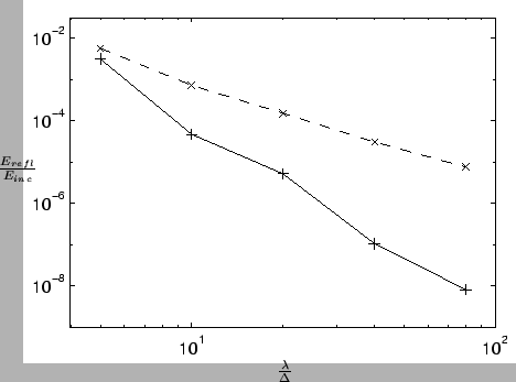 |
We also show some numerical results, comparing the numerical reflection error of the density doubling and quadrupling layers for normally incident waves. Waves (one period of a raised cosine) impinge on the layer from the side of smaller grid density (region ![]() ) in both cases. In Figure 4.40, we have plotted the log of the ratio of the reflected energy to the incident energy (
) in both cases. In Figure 4.40, we have plotted the log of the ratio of the reflected energy to the incident energy (
![]() ) versus the log of the number of grid spacings
) versus the log of the number of grid spacings ![]() per wavelength
per wavelength ![]() .
. ![]() and
and ![]() were computed by taking the sum of the squares of the junction quantities
were computed by taking the sum of the squares of the junction quantities ![]() over region
over region ![]() , before and after the passage of the wave through the interface.
, before and after the passage of the wave through the interface.
The density doubling layer (solid line in Figure 4.40) leads to a smaller reflected energy than the quadrupling layer (dashed line). This is to be expected--in general, the more abrupt a change in grid density, the more numerical reflection will result. As exemplified by Figure 4.40, however, the reflected energy will always tend to zero as grid density is increased on both sides of the interface. The case of oblique incidence has not been examined; it would appear, also, to be possible to derive an analytic expression for the numerical reflectance, though we have not done so here.
It would be very interesting to know whether the coarse/fine mesh arrangements discussed in this section and the last could be made truly multi-rate--that is, could we have scattering operations which recur with period ![]() in the coarse mesh, and period
in the coarse mesh, and period
![]() in the fine mesh? As mentioned earlier, there are TLM structures which are capable of this, but they in general perform time-averaging of wave quantities which may render the interface non-passive [87,88].
in the fine mesh? As mentioned earlier, there are TLM structures which are capable of this, but they in general perform time-averaging of wave quantities which may render the interface non-passive [87,88].
We also note that because interfaces between grids operating at different rates by necessity correspond to multi-step methods, we may also see parasitic modes [176] appearing along the interface (though we are assured convergence in the limit as the grid spacing becomes small). A discussion of parasitic modes in MDWDFs appears in §3.9.2.