Next: Stability
Up: The (1+1)D Advection Equation
Previous: The (1+1)D Advection Equation
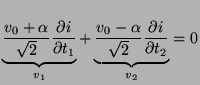
We first change coordinates via transformation (3.18), which gives
The basis of the WD integration approach is to view this equation as a loop equation for a multidimensional circuit, i.e., a circuit in which voltages and currents may depend not only on time but on space as well. The equation above is to be interpreted as describing a series connection of two inductors, where the dependent variable  is considered to be the current passing through them. The MD-inductors have inductances
As explained in §3.3, these two inductors are associated with the directions  and
and  . The circuit representation of the connection is shown in Figure 3.6(a).
Figure 3.6:
The (1+1)D advection equation-- (a) MDKC and (b) MDWD network.
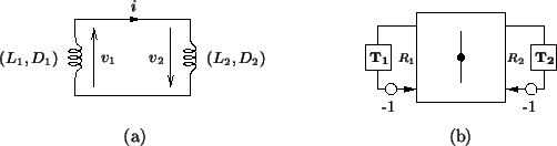 |
It is important to note that the circuit pictured here is merely a graphical representation of (3.51)--in particular, it represents the point-wise or differential behavior of (3.51) anywhere in the
 plane. It does, however, permit an immediate discretization via wave digital filters, in exactly the same manner as described in the previous chapter on lumped networks. That is, we can replace the circuit by two MDWD inductor one-ports connected through a series adaptor. This complete wave digital network is shown in Figure 3.6(b), where we have defined the port resistances to be:
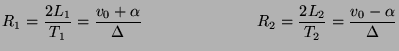 |
(3.50) |
where we have used
 .
Figure 3.6(b) is an abbreviated notation for a numerical integration routine. We can expand out the spatial dependence into a full signal flow graph in order to better perceive the flow of data. This is shown in Figure 3.7, where we have indicated unit time delays by
.
Figure 3.6(b) is an abbreviated notation for a numerical integration routine. We can expand out the spatial dependence into a full signal flow graph in order to better perceive the flow of data. This is shown in Figure 3.7, where we have indicated unit time delays by  ; series scattering junctions are separated by a distance
  .
.
Figure 3.7:
Signal flow graph for Figure 3.6(b).
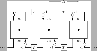 |
This signal flow graph can be interpreted as follows: At every grid point in the domain, and at every time step there are three computational stages:
- Retrieve the incoming wave variables from the registers. Referring to Figure 3.6(b), this means that for the port of port resistance
 , which accepts a wave variable shifted by
 , we must use the sign-inverted wave quantity output from the corresponding port, one time step earlier, and one grid point to the left. This shifting operation is to applied at every grid point, as per Figure 3.7. Similarly, the input to the port of port resistance
  takes the sign-inverted output of its corresponding port one time step earlier, and one grid point to the right.
- Perform scattering operation.
- Insert output wave variables into registers.
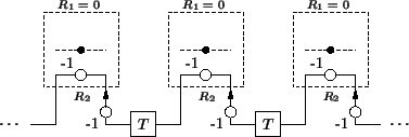
If
 , then either or is zero, depending on the sign of
  . In this case, the associated inductor can be dropped from the network entirely (i.e., we can treat it as a short-circuit). For example, if
  , then
implies that
, then
implies that  , and we get the simplified network of Figure 3.8. Here, we in fact have an exact solution to (3.51); the signals in the delay registers are shifted repeatedly to the left, and directly implement the traveling wave solution given by (3.53). Note that the sign inversion of the inductor is canceled by that of the reflection from the port.
Figure:
Simplified signal flow graph for Figure 3.6(b), for
,
.
 |
Next: Stability
Up: The (1+1)D Advection Equation
Previous: The (1+1)D Advection Equation
Stefan Bilbao
2002-01-22