Adsp-21369
Contents
- 1 Layout/Navigation of this WIKI page
- 2 Using the ADSP-21369 EZ-KIT Lite and Visual DSP++ Integrated Development Environment
- 3 Technical Specifications of the ADSP-21369 EZ-Kit Lite Development Board
- 4 Connecting the ADSP-21369 to the Visual DSP++ IDE
- 5 Topic: Using the AD1835A Codec Chip for DAC and ADC.
- 6 Topic: Memory Usage on the ADSP-21369.
- 7 Project: faust2sharc
- 8 How to use the faust2sharc generated C code
- 9 Resources
- 10 Project Members
- The first few sections of this page are devoted to getting you up and running on the ADSP-21369 EZ-KIT Lite and Visual DSP++ environment.
- There is a sample procedure on how to get an actual project running on the SHARC card.
- Next there are a few Special Topics outlining things we have found useful to know along the way. These topics can be viewed as a sort of FAQ when running into problems.
- Then there is a Project section explaining the "faust2sharc" program we have developed to convert Faust code to working c code that can be implemented on the SHARC card.
- Finally some useful links and resources are listed followed by a list of members working on this project so far.
NOTE: we encourage as many people as possible to continue to develop and improve the project we have begun. If you find any errors or underdocumented sections feel free to update them and document the changes. This is an open ended project devoted to helping as many people as possible get experience with on board DSP programming.
Using the ADSP-21369 EZ-KIT Lite and Visual DSP++ Integrated Development Environment
Through our friends at Analog Devices, Inc., CCRMA is now in posession of a few Analog Devices development boards (sometimes called 'Evaluation Kits'). At the current time, these include two ADSP-21369 EZ-KIT Lite development boards using SHARC processors, along with one ADSP-BF561 EZ-KIT Lite development board using the Blackfin processor. The purpose of this wiki is to serve as a resource of information for CCRMA students interested in using these development boards for projects involving audio signal processing. At the moment only the SHARC boards have been used, so the focus lies solely on them. Hopefully information on using the Blackfin board will come in turn.
Firstly, the technical specifications for the EZ-KIT Lite boards will be given, along with pointers to the manuals and data sheets provided for the specific hardware and software being used. Next, a step-by-step guide will be given for interfacing the development boards with the VisualDSP++ IDE, which is currently installed on a Windows XP machine located in the MaxLab. An modified version of one of the example projects is provided, containing comments and annotations that will hopefully be useful to the novice user. Afterwards, specials topics are discussed which might be useful to the beginning user, and DSP projects both begun and proposed are described, including a project which converts code written in the Faust language into a project file for the VisualDSP++ IDE.
The reader of this wiki is assumed to be familiar with programming in C/C++, as well as familiar with general digital signal processing theory. However, no prior experience with dedicated DSP hardware nor embedded systems is required, and in fact it is assumed that the reader is entirely unacquainted with the field. It is hoped that this wiki will continue to grow as more people use the boards for their audio processing projects, with each new project contributing its own formulated hints as to how one might get the best results when using this hardware.
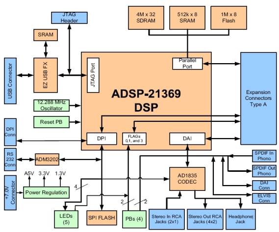
Technical Specifications of the ADSP-21369 EZ-Kit Lite Development Board
The following is a brief description of the hardware contained on the ADSP-21369 board, as well as the software used to program it. For a more detailed description, the reader is referred to the EZ-Kit Lite Manual
-The main DSP processing is performed by a SHARC processor, based on a 32-bit super Harvard architecture, with a core clock speed of 400 MHz.
-Audio I/O inteface:
- 4x2 RCA phono jacks for 4 channels of stereo output
- 2X1 RCA phono jacks for 1 channel of stereo input
- 3.5mm headphone jack for 1 channel of stereo output
- RCA phono jack input and output for SPDIF digital input and output
-The digital-to-analog and analog-to-digital conversion is performed by a single AD1835A codec chip:
- 4 stereo digital-to-analog converters (DACs)
- 1 stereo analog-to-digital converter (ADC)
- input/output sample-rates of up to 96 kHz on all channels
- 192 kHz sample-rate on one of the DAC channels
-The memory is broken up into multiple sections. The flash memories can store user-specific boot code, allowing the board to run as a stand-alone unit.
- 1M x 32-bit x 4 banks of synchronous dynamic random access memory (SDRAM)
- 512 Kbit x 8-bit synchronous random access memory (SRAM)
- 1M x 8-bit flash memory
- 2 Mbit serial peripheral interface (SPI) flash memory
-Universal asynchronous receiver/transmitter (UART):
- ADM3202 RS-232 driver/receiver
- DB9 female connector
-11 LEDs: 1 power (green), 1 board reset (red), 1 USB monitor (amber), and 8 general purpose (amber). 5 push buttons: 1 reset, 2 connected to DAI,2 connected to the FLAG pins of the processor.
-USB connection for interfacing with a computer.
-VisualDSP++ 5.0 integrated software development and debugging environment for Windows XP, allows programming of the board in assembly, C, and C++ (as well as combinations thereof), with various tools for project management and debugging.
-VisualAudio 2.5 audio software development tools and libraries, works in conjunction with VisualDSP++. Provides a set of graphical tools for developing audio processing data-flows, using a block-diagram approach. Contains tools for analysis, as well as the ability to treak the parameters of an algorithm in real-time. Comes with a collection of pre-built examples of various audio effects.
https://cm-wiki.stanford.edu/mediawiki/images/1/1f/ADSP-21369_Architecture.jpg
Connecting the ADSP-21369 to the Visual DSP++ IDE
There is currently one, and soon to be a second, Windows XP machine located in the MaxLab which has both the VisualDSP++ and VisualAudio software already installed, as well as the hardware drivers necessary for interfacing with the ADSP-21369. It is the purpose of this section to give a step-by-step guide for connecting the board to the computer, interfacing with the VisualDSP++ IDE, and loading an example audio-processing project onto the board. As a first step, the interested student should get in touch with Carr Wilkerson (carrlane at ccrma), who knows where the EZ-KITs are located and will be happy to set up a new account on the Windows machine. Once those two things are taken care of, connecting the board to the computer goes as follows:
- Getting Started
- Log into the Windows computer (the keyboard and monitor for the machine are shared with a neighboring Linux machine, so you may have to use the switch next to the monitor to get to Windows).
- Plug in the USB cable connected to the back of the Windows machine into the ADSP-21369.
- Note: Make sure that the LED next to the USB plug of the ADSP-21369 is lit up. This shows that the board is properly communicating with the computer
- From the Start Menu, open up 'Visual DSP++ Programming Environment'.
- At the top of the window you should see “[Target: ADSP-21369 EZ-KITLite via Debug Agent]” Which means you are properly connected to the board and are ready to program.
- Note: If it doesn’t say you are connected to a target click the “Connect to Target” button
- Running a Project
- Download and unzip the "DelayLine" folder
- Connect an audio source to the RCA input channel labeled “Audio In” on the board
- Connect your speakers to the Channel One Audio Outputs or the 1/8th Inch Stereo Headphone Jack
- In the Visual DSP++ Environment, choose “File->Open->Project” from the menu bar, navigate to the “DelayLine” folder and open the Visual DSP++ Project file
- Choose “Project->Build Project” (F7) from the menu bar to build the project
- Once it is finished building, choose “Debug->Run” (F5) from the menu bar in order to load the program onto the board and run it
- You should now hear the Audio Input with a feedback delay
- Other example projects
High Pass Filter (C code)
Freeverb (Faust file and faust2sharc generated C code)
Topic: Using the AD1835A Codec Chip for DAC and ADC.
The ADSP-21369 EZ-KIT Lite uses a single AD1838A sigma-delta codec chip for performing ADC and DAC functions. An understanding of how this chip works is imperative when developing projects for the ADSP-21369. Much helpful information can be found by reading the data sheet for the AD1835A.
One particular important bit of information is found on page 11: "The DAC and ADC output data stream is in a twos complement encoded format. The word width can be selected from 16 bit, 20 bit, or 24 bit." This means that the sample data delivered from the ADC will be in twos complement form such that, if one if developing an audio-processing project in VisualDSP++ using C, an appropriate sign extension will be required before processing the data in the usual way. Additionally, the word width must be specified somewhere in the initialization portion of the project.
While a detailed listing of the register addresses used by the AD1835A is contained in data sheet, it might be quicker and more intuitive to inspect some project code which initializes the codec chip and transmits/receives sample data to/from it. For instance, looking at the example project from the previous section, one immediately notices multiple files with '1835' in their names. The header file 'ad1835.h' contains definitions for the various register addresses and settings on the codec chip. The file 'init1835viaSPI.c' contains functions for communicating with the AD1835A using the SPI, in order to initialize the chip with the desired settings. The array 'Config1835Param[]' contains the settings, while the function 'Init1835viaSPI()' performs the initialization. The code, originally from the 'Block Based Talkthrough (C)' example supplied with VisualDSP++, is helpfully commented.
Topic: Memory Usage on the ADSP-21369.
The below material was referenced directly from the ADSP-2136x SHARC Processor Programming Reference linked at the bottom of the page
Super Harvard Architecture: Most microprocessors use a single address and a single-data bus for memory accesses. This type of memory architecture is referred to as the Von Neumann architecture. Because processors require greater data throughput than the Von Neumann architecture provides, many processors use memory architectures that have separate data and address buses for program and data storage. These two sets of buses let the processor retrieve a data word and an instruction simultaneously. This type of memory architecture is called Harvard architecture.
SHARC processors go a step further by using a Super Harvard architecture. This four bus architecture has two address buses and two data buses, but provides a single, unified address space for program and data storage. While the data memory (DM) bus only carries data, the program memory (PM) bus handles instructions and data, allowing dual-data accesses.
Memory: The ADSP-2136x processors are comprised of two groups, the ADSP-21362/3/4/5/6 and the ADSP-21367/8/9 processors. The differences in these group’s memory is the ADSP-21367/8/9 processors contain an external port which is made up of an asynchronous memory interface, an SDRAM controller and, in the case of the ADSP-21368, a shared memory interface. Also, the processor groups have different amounts of ROM/RAM memory.
While each memory block can store combinations of code and data, accesses are most efficient when one block stores data using the DM bus, for transfers, the second block stores instructions and data using the PM bus and a third and fourth block stores data using the I/O bus. Using the DM and PM buses in this way assures single-cycle execution with two data transfers. In this case, the instruction must be available in the cache.

Project: faust2sharc
We (or, more precisely Andrew, A.K.A the captain of the A-TEAM), developed a script which takes in Faust code (on .dsp format), and returns C code, ready to plug into VisualDSP++. The script is called faust2sharc, release 0.0.2 can be downloaded from here.
When modifying a code or trying out new code, it is recommended that you make sure your Faust code definitely compiles as such, by for example generating a C++ code or a block diagram using Faust.
Instructions on running faust2sharc
- Download and install faust2sharc from the link above.
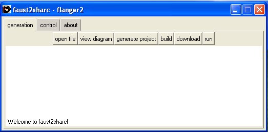
- The interface should look like this:
- https://cm-wiki.stanford.edu/mediawiki/images/c/c5/Faust2sharc_small_blank.jpg
- Upload the [name_of_file].dsp file with the open file button.
- Press generate project. This generates a [name_of_file].c file.
- Upload the [name_of_file].c file to VisualDSP++.
- The Faust generated block diagrams can be viewed by pressing on the view diagram button. This generates a folder in your workspace called [name_of_file].dsp-svg which includes block diagrams for the project.
How to use the faust2sharc generated C code
- Open the faust2sharc VisualDSP++ template project file.
- Right click on the Source Files folder and and select "Add file(s) to folder.." Select the faust2sharc generated c code file.
- Under the Linker Files folder, right click faust2sharc.ldf and select "open with source window"
- In the ldf file, on line 222, change the line "xxx.doj(seg_dmda)" to the new name of the added file. For example, if the faust2sharc generated c code has a filename of "food.c", then change line 222 to "food.doj(seg_dmda)"
- Rebuild project and you are done!


Resources
Analog Devices Resources
- Manuals for Relavent AD Products
- ADSP-21369 SHARC EZ-KIT Lite Evaluation Kit Product Description
- ADSP-2136x SHARC Processor Programming Reference
- ADSP-2136x SHARC Processor Hardware Reference
Faust Resources
Project Members
- Steinunn Arnardottir
- Andrew Best
- Baek San Chang
- Turner Kirk
- Kyle Spratt