


Next: Type I: Voltage-centered Network
Up: Transverse Motion of the
Previous: Finite Differences
Waveguide Network for the Euler-Bernoulli System
It is possible to design a waveguide network which simulates the behavior of equation (5.1), but there are some extra features we must add which were not necessary in the case of the transmission line. In addition, the overloaded symbols for the wave variables become even more overloaded, due to the fact that we can no longer interleave the two dependent variables spatially, and are faced with a double set of wave variables at every grid point. (This can be remedied with recourse to other more involved difference methods, but we will not pursue this subject here.) The structure of interest is shown in Figure 5.1.
Figure 5.1:
(1+1)D DWN for the Euler-Bernoulli system (5.4).
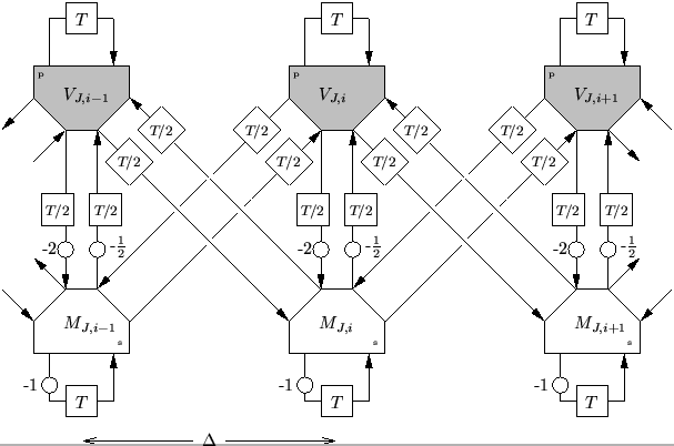 |
This is still a (1+1)D waveguide network, like that which simulates the (1+1)D transmission line equations, but we have drawn the junctions which calculate  and
and  separately; it should be kept in mind that they operate at the same spatial locations. As before, we use grey/white coloring of junctions to signify operation at different time steps. Here we have interpreted (which we will identify with
  of difference scheme (5.5), and thus with
  ) as a voltage-like variable, and as the current-flow. Also as before, the diagram above is correct when we are using voltage-like wave variables as our signals. Figure 5.2 gives the complete picture of the wave quantities and immittances in the network.
Figure 5.2:
Scattering junctions of Figure 5.1, with incoming and outgoing voltage waves indicated.
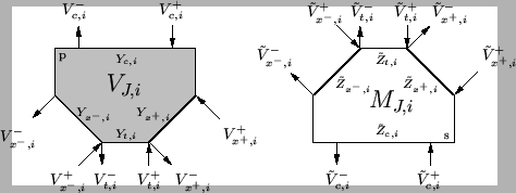 |
We note that the wave variables at the series scattering junction at location  are indicated by a tilde, to distinguish them from those at the parallel junction at the same location, even though the two sets of variables are calculated at alternate time steps. As for the (1+1)D transmission line, we index wave variables and immittances at the left and right ports of any junction by
  and
and  respectively, and the same such quantities associated with any self-loop are subscripted with
  . We also have new waveguides connecting parallel and series junctions at the same grid point; immittances and wave variables are subscripted with a
  in this case. With reference to Figure 5.2, we can define the junction admittance at the parallel junction, and the junction impedance at the series junction to be
It should be clear that this waveguide network is really a pair of coupled (1+1)D transmission lines; the coupling is via the waveguide connecting the series and parallel junctions at the same grid location (the vertical waveguide in Figure 5.1).
Figure 5.3:
An equivalent form for duplicate bidirectional delay lines running between a parallel and a series junction.
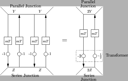 |
The factors of -2 and
 in the ``coupling'' waveguide in Figure 5.3 deserve some extra commentary. Figure 5.3 shows an equivalence between two waveguide configurations. On the left, we have two identical waveguides with delay
  time steps and impedance
  connected between a parallel junction and a series junction; in approximating a second derivative by centered differences, as we are indeed doing in (5.5), we need such a configuration so as to double the strength of the wave variable coming from the same grid location at the previous time step relative to that of those entering from the neighboring junctions. The equivalent form on the right, which introduces a transformer with turn ratio -2, serves to reduce the pair of waveguides to a single one, accompanied by two multiplications (the waveguide transformer is identical to the wave digital transformer, discussed in §2.3.4). This implies that the port impedance
  at a parallel junction at grid point
  in Figure 5.1 and the port admittance
 at the series junction at the same point must be related by
 |
(5.9) |
(This equivalence can easily be derived through the manipulation of hybrid matrices for bidirectional delay lines, as per the methods discussed in §4.10.2.) Also note the sign inversions in this central coupling waveguide with respect to the left- and right-going waveguides.
We now trace the signal flow in the network to show that it does indeed solve the Euler Bernoulli system. Beginning from a series junction at grid point , we have:
which is identical to (5.5b) if we replace by and by  , and if we have
 |
(5.10) |
Beginning from the series junction, we arrive at a similar requirement for  , namely
 |
(5.11) |
As in the case of the transmission line, three families of waveguide networks are distinguishable:
Subsections
Next: Type I: Voltage-centered Network
Up: Transverse Motion of the
Previous: Finite Differences
Stefan Bilbao
2002-01-22