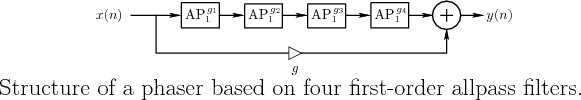
The block diagram of a typical inexpensive phase shifter for
guitar players is shown in Fig. 1.5It consists of a
series chain of first-order allpass filters,6 each having a single
time-varying parameter ![]() controlling the pole and zero location
over time, plus a feedforward path through gain
controlling the pole and zero location
over time, plus a feedforward path through gain ![]() which is a fixed
depth control.
which is a fixed
depth control.
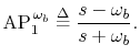
In analog hardware, the first-order allpass transfer function [#!JOSFP!#, Appendix C, Section 8]7is
Classic Analog Phase Shifters
Setting ![]() in Eq.
in Eq.![]() (4) gives the frequency response of the analog-phaser
transfer function to be
(4) gives the frequency response of the analog-phaser
transfer function to be
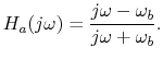
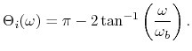
Figure ![]() a shows the phase responses of four first-order analog allpass
filters with
a shows the phase responses of four first-order analog allpass
filters with ![]() set to
set to
![]() .
Figure
.
Figure ![]() b shows the resulting normalized amplitude response for the phaser, for
b shows the resulting normalized amplitude response for the phaser, for ![]() (unity feedfoward gain). The amplitude response has also been
normalized by dividing by 2 so that the maximum gain is 1. Since
there is an even number (four) of allpass sections, the gain at dc is
(unity feedfoward gain). The amplitude response has also been
normalized by dividing by 2 so that the maximum gain is 1. Since
there is an even number (four) of allpass sections, the gain at dc is
![]() . Put another way, the initial phase of each allpass
section at dc is
. Put another way, the initial phase of each allpass
section at dc is ![]() , so that the total allpass-chain phase at dc is
, so that the total allpass-chain phase at dc is ![]() .
As frequency increases, the phase of the allpass chain decreases. When it comes
down to
.
As frequency increases, the phase of the allpass chain decreases. When it comes
down to ![]() , the net effect is a sign inversion by the allpass chain, and the
phaser has a notch. There will be another notch when the phase falls down to
, the net effect is a sign inversion by the allpass chain, and the
phaser has a notch. There will be another notch when the phase falls down to ![]() .
Thus, four allpass sections give two notches. For each notch in the desired
response we must add two new allpass sections.
.
Thus, four allpass sections give two notches. For each notch in the desired
response we must add two new allpass sections.
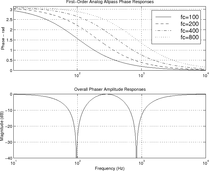
From Fig. ![]() b, we observe that the first notch is near
b, we observe that the first notch is near ![]() Hz. This happens to be the frequency at which the first allpass pole
``breaks,'' i.e.,
Hz. This happens to be the frequency at which the first allpass pole
``breaks,'' i.e.,
![]() . Since the phase of a first-order
allpass section at its break frequency is
. Since the phase of a first-order
allpass section at its break frequency is ![]() , the sum of the
other three sections must be approximately
, the sum of the
other three sections must be approximately
![]() .
Equivalently, since the first section has ``given up''
.
Equivalently, since the first section has ``given up'' ![]() radians
of phase at
radians
of phase at
![]() , the other three allpass sections
combined have given up
, the other three allpass sections
combined have given up ![]() radians as well (with the second
section having given up more than the other two).
radians as well (with the second
section having given up more than the other two).
In practical operation, the break frequencies must change dynamically, usually periodically at some rate.
Classic Virtual Analog Phase Shifters
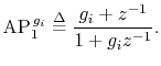
To create a virtual analog phaser, following closely the design
of typical analog phasers, we must translate each first-order allpass
to the digital domain. Working with the transfer function, we must
map from ![]() plane to the
plane to the ![]() plane. There are several ways to
accomplish this goal [#!RabinerAndGold!#]. However, in this case,
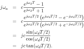
an excellent choice is the bilinear transform (see §
plane. There are several ways to
accomplish this goal [#!RabinerAndGold!#]. However, in this case,
an excellent choice is the bilinear transform (see §![]() ),
defined by
),
defined by
Thus, given a particular desired break frequency
![]() , we can set
, we can set
Recall from Eq.![]() (4) that the transfer function of the
first-order analog allpass filter is given by
(4) that the transfer function of the
first-order analog allpass filter is given by
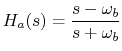
where we have denoted the pole of the digital allpass by
Figure ![]() shows the digital phaser response curves corresponding to the analog
response curves in Fig.
shows the digital phaser response curves corresponding to the analog
response curves in Fig. ![]() . While the break frequencies are
preserved by construction, the notches have moved slightly, although
this is not visible from the plots. An overlay of the total phase of
the analog and digital allpass chains is shown in Fig.
. While the break frequencies are
preserved by construction, the notches have moved slightly, although
this is not visible from the plots. An overlay of the total phase of
the analog and digital allpass chains is shown in Fig. ![]() .
We see that the phase responses of the analog and digital alpass
chains diverge visibly only above 9 kHz. The analog phase response
approaches zero in the limit as
.
We see that the phase responses of the analog and digital alpass
chains diverge visibly only above 9 kHz. The analog phase response
approaches zero in the limit as
![]() , while the digital
phase response reaches zero at half the sampling rate,
, while the digital
phase response reaches zero at half the sampling rate, ![]() kHz in
this case. This is a good example of when the bilinear transform
performs very well.
kHz in
this case. This is a good example of when the bilinear transform
performs very well.
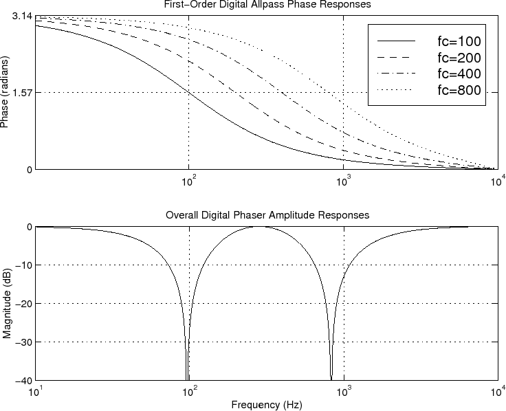
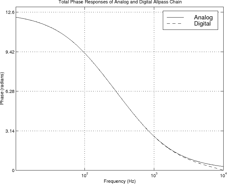
Fig. ![]() below 10 kHz can be largely eliminated by increasing
the sampling rate by 15% or so. See the case of digitizing the Moog
VCF for an example in which the presence of feedback in the analog
circuit leads to a delay-free loop in the digitized system
[#!StilsonAndSmithMoogVCF!#,#!StilsonT!#].
below 10 kHz can be largely eliminated by increasing
the sampling rate by 15% or so. See the case of digitizing the Moog
VCF for an example in which the presence of feedback in the analog
circuit leads to a delay-free loop in the digitized system
[#!StilsonAndSmithMoogVCF!#,#!StilsonT!#].